


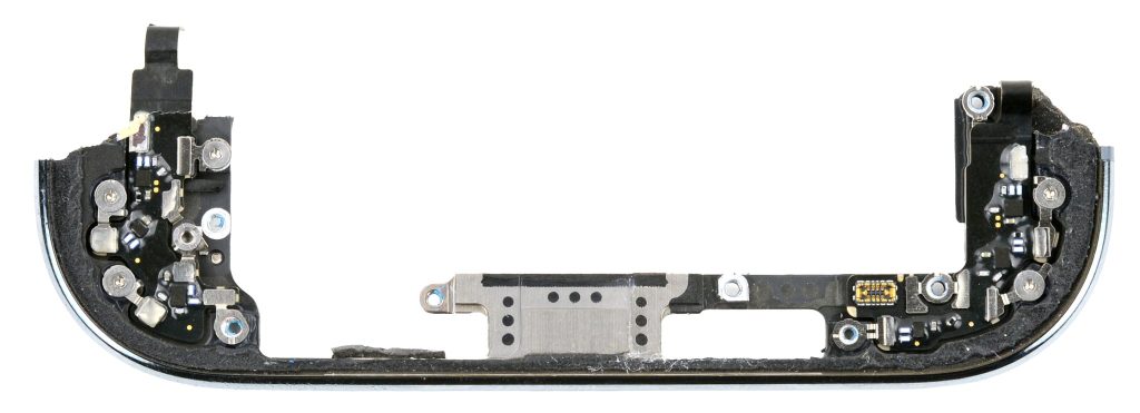
When we disassembled Apple’s thinnest-ever handheld computer, we were amazed by its exquisite engineering design. At just 5.6 millimeters thick, it was surprisingly easy to repair. Even more surprising was that the MagSafe charger used the same battery as the phone itself (and they were interchangeable!). The initial excitement may have faded, and if reports of production cuts are true, that enthusiasm may have waned considerably.
But our microscopic analysis of the iPhone Air’s 3D-printed USB-C connector has caused a minor stir in the metal 3D printing world. Over the past six weeks, we’ve spoken with numerous additive manufacturing experts, and Apple has confirmed some of our key findings. Now it’s time to share them with you.
So, how did they do it? How was the first 3D-printed iPhone component manufactured?
A small port, but a big fuss.
When the EU standardized charging ports for electronic devices, we and the rest of the world cheered. But when we disassembled the phones and examined the connectors closely, our main concern was whether they were modular: could they be replaced if damaged?
In this case, well, sort of. It’s quite complicated, much more so than ideal.
However, this time, Apple is telling us to take a closer look at the connector: its casing is 3D printed using recycled titanium metal by a laser powder bed fusion printer from BLT. This additive manufacturing process was launched simultaneously with the 3D printed titanium casings of the Apple Watch Series 11 and Ultra 3.
It’s exciting to see 3D printing technology finally being used for such large-scale production. This shift to 3D printing also brings significant benefits for those of us who are sustainability enthusiasts: Apple reports that the process saves 33% to 50% in material consumption compared to traditional forging methods. At a time when overconsumption is a major concern, efficient resource utilization is undoubtedly a welcome development.
The mystery of crop circle pattern
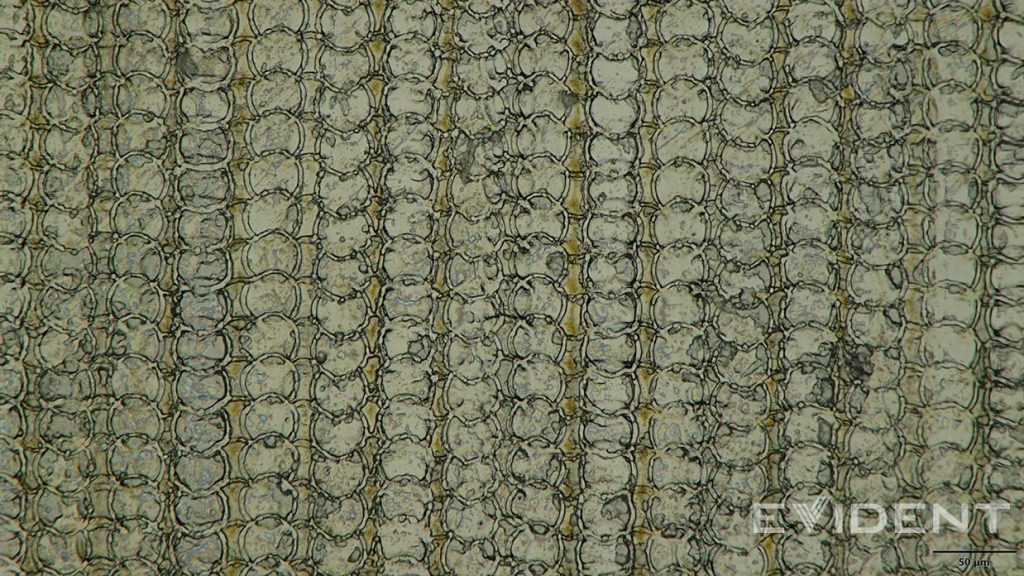
After disassembling the iPhone Air, we examined the USB-C connector using an Evident DSX2000 microscope. The magnified image of the USB-C connector revealed a perplexing detail: a chain-like circular surface pattern that even experienced 3D printing experts couldn’t explain. At a scale of 50 micrometers, this pattern appears extremely unusual.
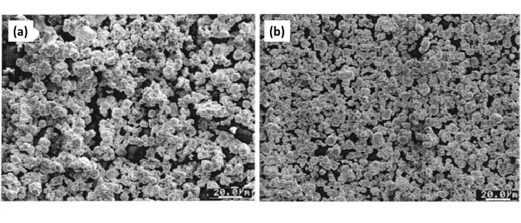
Early reports suggested that Apple might be using binder jetting technology, a 3D printing process that combines powder with a binder (which acts as an adhesive). Two years ago, when it was first reported that Apple was experimenting with 3D printing for Apple Watch cases, a Chinese company called EasyMFG showcased a smartwatch case printed using binder jetting technology.
However, under a microscope, the patterns produced by the binder jetting process are far less regular than the crop circle-like patterns we observed on the USB-C connector housing. Therefore, our industry sources suspect that what we saw was not the binder jetting process.
Here I need to make a crucial clarification: despite the interesting similarities between the two, the USB-C interface does not possess antibacterial properties. The circular structures we see, with a diameter of approximately 30 micrometers, are not small enough; as relevant research shows, indentations on the 5-10 micrometer scale are needed to effectively repel bacteria.
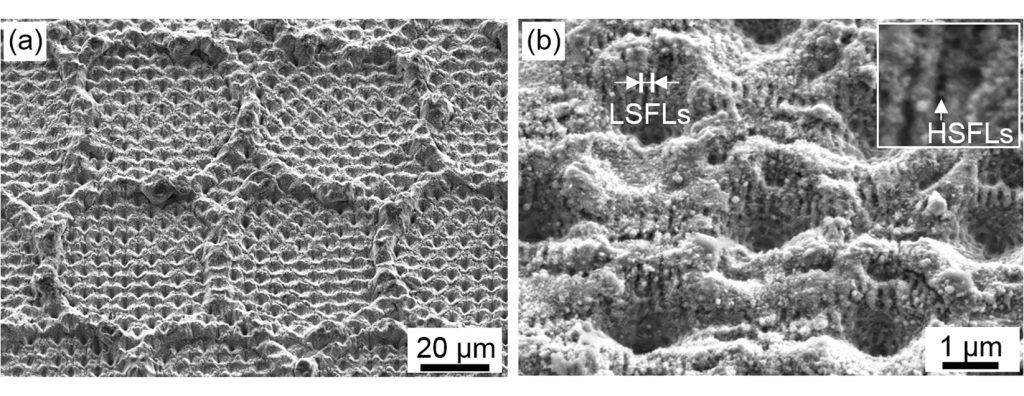
However, the similar patterns and dimensions, while not conclusive evidence, suggest the possible use of pulsed laser technology. Furthermore, the images show subsurface layer contours with the same pattern, indicating that the technology was used throughout the entire printing process, not just on the outer layer.
As expected, Apple published an article yesterday describing their process: countless machines, each equipped with six lasers, stacking 900 layers of titanium to create each Apple Watch case. While the article didn’t explicitly mention “pulsed laser ablation,” its description confirms our experts’ conclusions.
Editor’s Note: Based on our images, our experts believe the process is pulsed laser ablation, a subtractive process that removes material to form the final shape; additive manufacturing, on the other hand, refers to laser melting, a process that builds components from scratch.
Why might Apple choose pulsed laser ablation technology?
Apple’s article emphasized the environmental benefits of 3D printing with titanium and directly linked this choice to the company’s goal of achieving carbon neutrality by 2030.
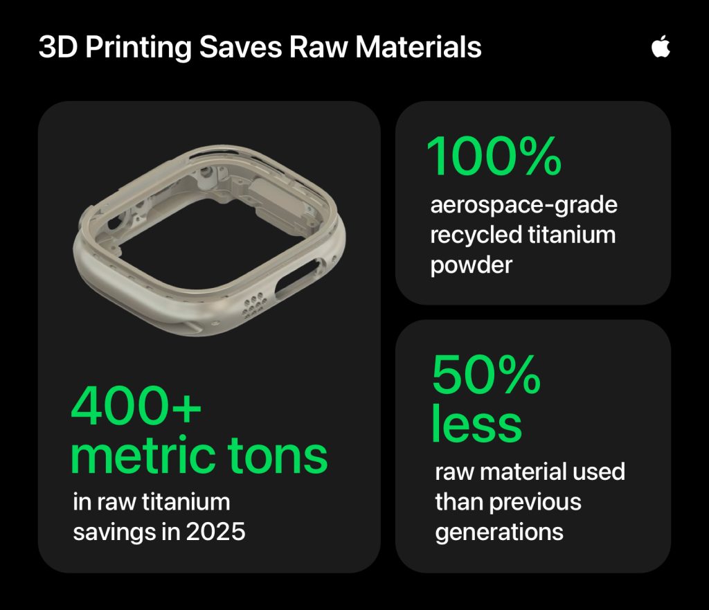
This year, using printing instead of stamping will save them over 400 tons of titanium raw materials, which is a significant portion of their annual titanium consumption of 7,000 tons. The environmental benefits of reducing metal mining and production waste are obvious, and the economic benefits are also considerable: the titanium market has always been unstable, and since most titanium processing takes place in China, the price of titanium is affected by the constantly changing tariff environment.
However, pulsed laser ablation technology has some other advantages that may be very attractive for the iPhone Air and Apple Watch Series 11 and Ultra 3.
It’s not that hot anymore.
Short pulses (typically in the nanosecond to femtosecond range) minimize heat diffusion, preventing deformation or discoloration when melting 50-micron titanium powder particles. Discoloration might be insignificant for the tiny components inside the iPhone Air, but it’s crucial for the Apple Watch casing.
Apple’s article mentions that controlling heat by refining recycled titanium to create a low-oxygen mixture is necessary; using micropulse vaporization of titanium alloy powder may provide them with another method to control the transfer of laser energy to the heat-sensitive titanium alloy powder.
It can create useful surface treatment effects.
This micro-texture, similar to crop circles, may play a role in the assembly process of the iPhone Air. It could potentially enhance the adhesion of waterproof seals or coatings around the ports.
In fact, Apple lists this advantage as one of the core features of the 3D-printed titanium material used in the Apple Watch. They state that their process allows them to…
“Improve the waterproofing of the antenna housing on cellular models. The cellular model’s housing has a plastic-filled compartment inside to accommodate the antenna function, and by 3D printing a specific texture on the inner surface of the metal, Apple achieves better adhesion between the plastic and the metal.”
It’s easy to imagine that the USB-C port could also benefit from a similar approach.
It’s very precise.
Pulsed lasers can engrave or texture metal surfaces with sub-micron precision, making them ideal for processing the delicate components around USB-C ports or for cleaning post-welding areas. Given the extremely high precision requirements of the iPhone Air to achieve its 5.6 mm thin profile, Apple seems to have recognized the precision capabilities of pulsed laser ablation technology for the dimensions of both the USB-C port housing and the Apple Watch casing.
It’s very efficient.
Another paper, authored by Henriques et al. (also from the medical field), demonstrates the application of ultrashort pulse technology as a fast and efficient manufacturing method. Considering the potential for this technology to be used in the mass production of components for one of the best-selling products in human history (the iPhone has outsold the Toyota Corolla, though it still lags behind classics like wheat and the Bible), adopting this process, which is more energy-efficient, faster, and utilizes materials more effectively, becomes particularly important.
Unveiling the mystery of “aerospace-grade” titanium.
The investigation also yielded another interesting finding: the specific grade of titanium alloy used by Apple. Apple’s marketing team calls it “aerospace-grade” titanium alloy, but this is not the actual grade of the alloy.
This claim may be somewhat misleading, as X-ray fluorescence (XRF) analysis shows that while the alloy is based on T6Al4V (one of several “aerospace-grade” titanium alloys), the use of ferrochrome means it is not the alloy typically used in aerospace applications. The use of chromium makes the alloy brittle at high temperatures, and the iron content reduces its corrosion resistance—both undesirable characteristics in aerospace applications.
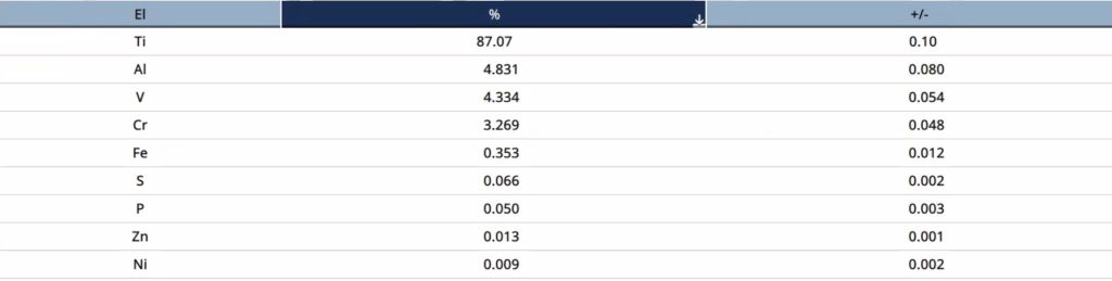
Even more interestingly, this ferrochrome element is apparently a byproduct of the titanium recycling process. According to one of our industry experts, this suggests that Apple is recycling titanium waste generated during its manufacturing process, adding ferrochrome to create this unique custom alloy suitable for 3D printing, and then upcycling this modified titanium for use in other products.
Undoubtedly, this custom USB-C connector is an engineering marvel. We suspect the primary motivation behind its existence is to ensure supply chain stability—thereby mitigating the volatility of the global titanium market—but the resulting reduction in material waste is also a welcome byproduct.
How can this change be reversed?
Many repair enthusiasts are excited about the potential of 3D printing to transform the industry: if people can print spare parts at home, manufacturers won’t need to stockpile vast quantities of parts in warehouses. We also wouldn’t have to waste energy and money shipping parts globally. People could get parts instantly when needed. Philips is working towards this vision, and although progress is slow, they have already made printing files for two parts of their shavers available on the Printables website.
However, this isn’t the case with Apple. Apple hasn’t provided any printing files. Even if they did, given the materials involved and the highly specialized nature of the process, it would be difficult for users with home 3D printers to utilize them. Furthermore, the 3D-printed titanium USB-C enclosure is tightly bonded to other components, and the Apple Watch case itself isn’t easily damaged.
In short: how can this change make up for the shortcomings? It can’t.
3D printing technology holds the promise of revolutionizing manufacturing, increasing efficiency, reducing carbon emissions, and easing the strain on the planet by reducing the need for mining. But for most parts and most manufacturers, this is somewhat out of reach. Very few manufacturers have the expertise and infrastructure required to implement such processes, let alone on a large scale. Even Apple is starting small: the USB-C connector enclosure is a tiny part in a low-volume product, making it ideal for experimentation.
Nevertheless, we can’t let the mystery of the crop circles go unsolved. Therefore, we are deeply grateful to the experts in the additive manufacturing industry who helped us explore the possibilities.